Special Interview: The “JOINT3” Consortium for Next-Generation Semiconductor Packaging
How High-Precision Metrology Enables the Future of Advanced Semiconductor Packaging
Source: Reprinted from Nikkei MOOK “Semiconductor Ecosystem – A New Era of Industry Driven by Global Collaboration” (Nikkei Publishing)


Mitutoyo, a global manufacturer of precision measuring instruments, is a participant in JOINT3, a collaborative research and development platform focused on next-generation semiconductor packaging. The initiative brings together 27 companies from Japan and around the world.
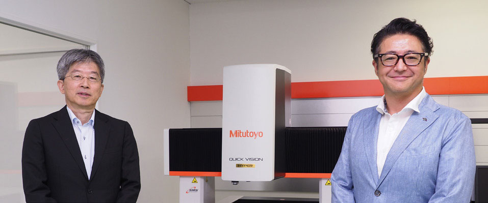
In this special dialogue, Abe Hidenori of Resonac, which leads the JOINT3 initiative, and Goto Tomonori of Mitutoyo discuss the significance of JOINT3 and the critical role precision metrology plays in advancing next-generation semiconductor packaging technologies.
Reliable Evaluation Data Is Essential for Advanced Technology Development
Abe Hidenori
Chief Technology Officer for Semiconductor Materials
Executive Director, Electronics Business Headquarters
Resonac
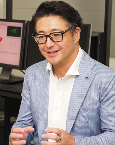

Creating New Measurement Technologies to Lead the Semiconductor Industry
Goto Tomonori
Senior Executive Officer
Head of Research & Development
Mitutoyo Corporation
Proven Expertise in Integrated Mechanical and Optical Technologies
2.xD semiconductor packaging refers to an architecture in which multiple semiconductor chips are placed side by side and interconnected through an interposer (intermediate substrate).
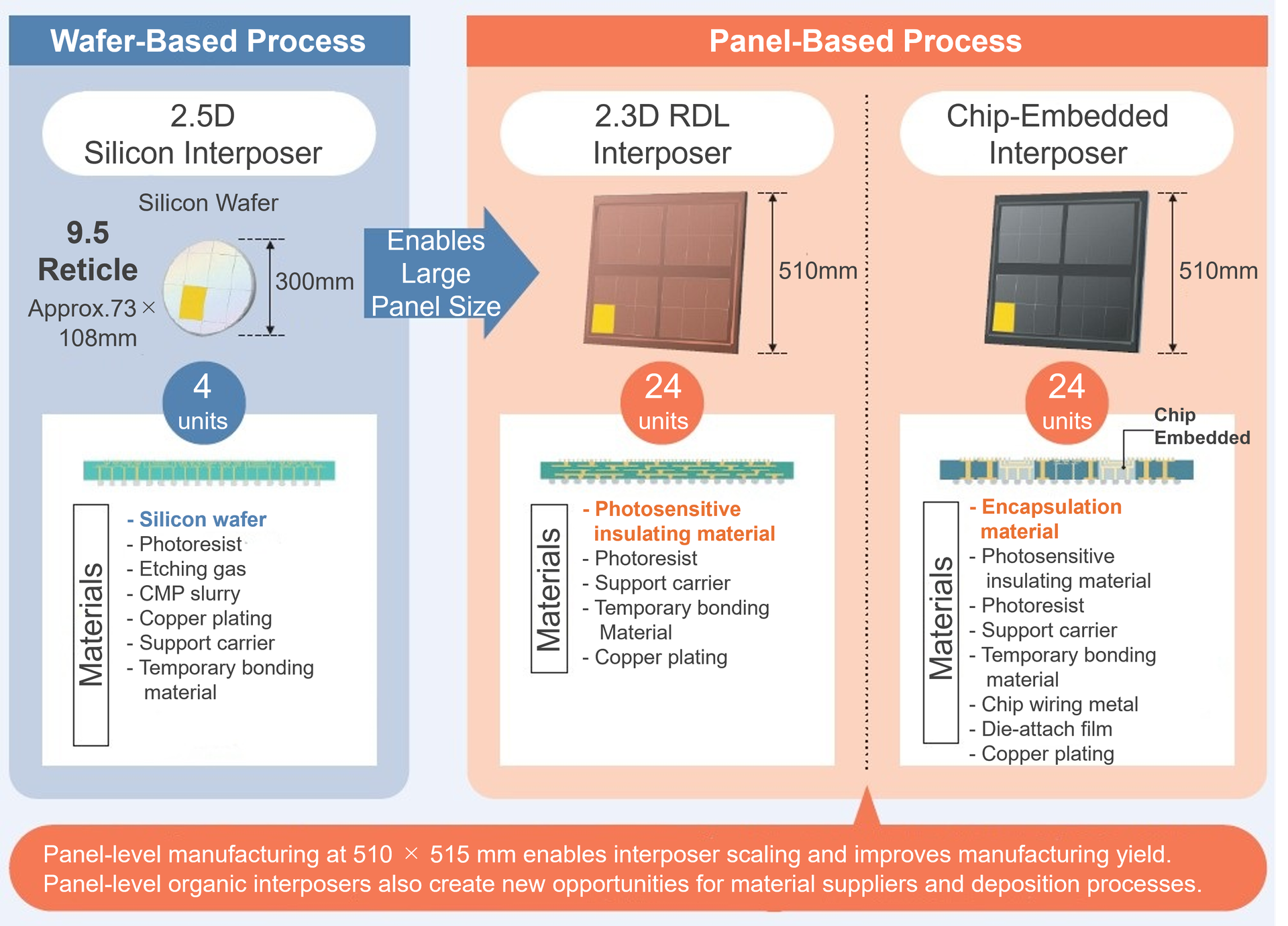
Recently, industry focus has shifted toward panel-level manufacturing. Instead of arranging chips on a circular wafer and dividing them after processing, this approach uses large square panels, enabling higher production efficiency and increased interposer output.
Figure 1: Evolution of Semiconductor Packaging—from Traditional Packaging to 2.5D Chiplet Integration
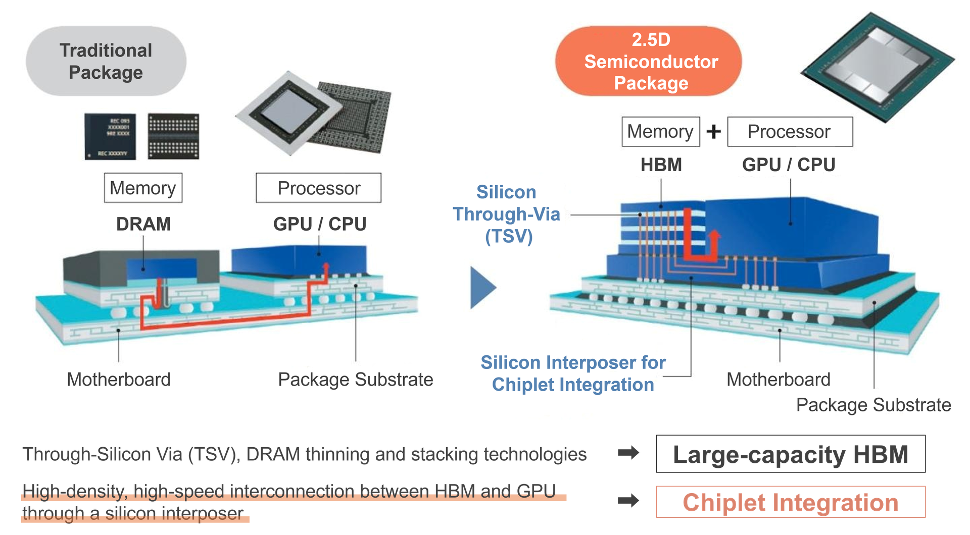
Within JOINT3, a next-generation semiconductor packaging R&D platform led by Resonac, participating companies are collaborating to establish a panel-level packaging evaluation line measuring 515 × 510 mm. This initiative aims to accelerate the development of materials, manufacturing processes, measurement systems, and assembly technologies required to support these advancements.
Figure 2: Transition from Wafer-Based to Panel-Level Interposer Manufacturing
Goto:
Resonac holds a number of products with leading global market share in semiconductor materials. Could you share the background behind establishing JOINT3 and the significance of this collaborative platform?
Abe:
Driving innovation both quickly and flexibly requires close collaboration between materials manufacturers and equipment manufacturers. In the advanced packaging field, companies with diverse core strengths have come together to address these challenges. Mitutoyo’s participation was a natural fit given its expertise in precision measurement.
Goto:
Mitutoyo has long developed and supplied precision measuring instruments used across a wide range of industries. We also design and manufacture our own optical lenses, enabling us to integrate mechanical engineering with advanced optical technologies. These capabilities are widely utilized not only in our own systems but also by many equipment manufacturers.
In the manufacturing of organic interposers, increasing substrate size can lead to challenges such as panel-edge warpage and variations in wiring and resin thickness. These factors make accurate measurement more difficult. Through JOINT3, we aim to build an evaluation and prototyping line that enables participating companies to assess these challenges collaboratively, share results, and reduce overall development costs.
Abe:
To date, JOINT3 has advanced technologies related to Fan-Out packaging and 2.xD (AI semiconductor) packaging. Moving forward, we aim to drive innovation in panel-level manufacturing, particularly in achieving large-area, high-density fine patterning.
Goto:
The 2.3D RDL interposer used in JOINT3 requires extremely fine wiring structures, with line/space dimensions of 1/1 μm. In addition, connecting multiple semiconductor chips requires technologies such as micro-bump bonding and via formation, which involve complex three-dimensional structures. For this reason, advanced 3D measurement technology is essential.
Mitutoyo has extensive experience in semiconductor packaging measurement and will contribute to JOINT3 by providing advanced, high-precision measurement solutions.
Abe:
Technologies such as SAP (Semi-Additive Process), in which copper is embedded into seed layers formed along wiring patterns, and mSAP (Modified Semi-Additive Process), which enables copper embedding in extremely fine wiring grooves, are also under development. These technologies are expected to enable line/space dimensions approaching 1/1 μm in the near future.
The semiconductor industry evolves rapidly and faces intense global competition. As new materials, manufacturing processes, and measurement technologies are continuously introduced, we expect JOINT3 participants to leverage this collaborative platform to develop innovations that may become de facto standards across the industry.
Pinpoint Measurement Using Infrared Transmission Imaging
In 2.xD semiconductor packages, which incorporate three-dimensional structures, inspection methods beyond visible-light observation are required to evaluate embedded components.
Goto:
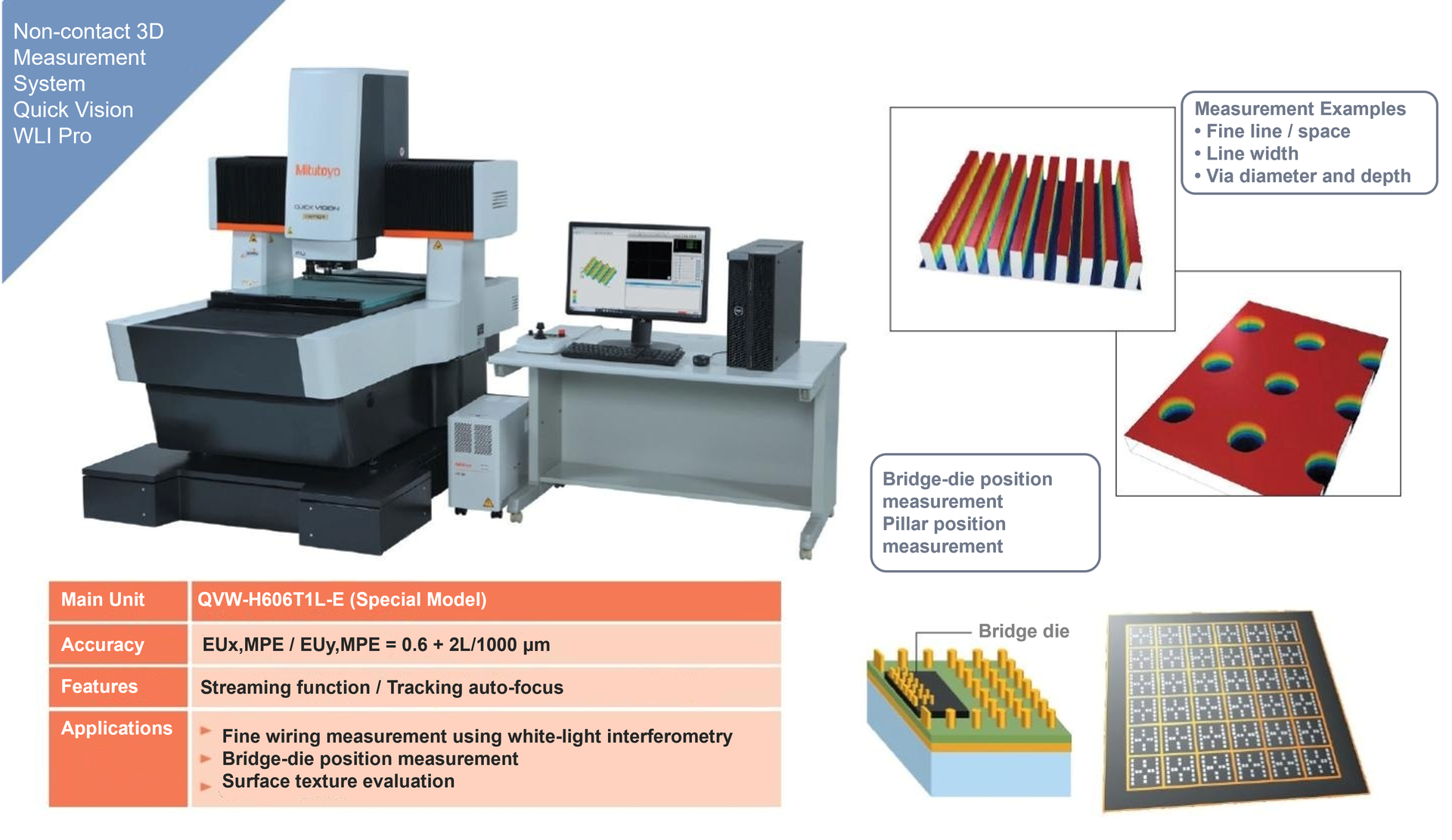
At the Advanced Panel Interposer Center (APIC) in Hitachinaka City, Ibaraki Prefecture, where JOINT3 activities are conducted, we have installed our non-contact 3D measurement system, the Quick Vision WLI Pro, along with the QV-IR HYPER 606.
The Quick Vision WLI Pro enables continuous measurement from features such as height and angles to advanced 3D analysis, including surface roughness, cross-sectional dimensions, and step height measurement. This allows for efficient evaluation of semiconductor packaging substrates.
Figure 3: Quick Vision WLI Pro Enables Efficient, Non-Destructive Large-Area Measurement
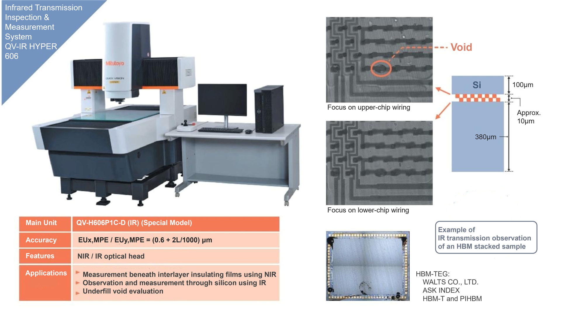
The QV-IR HYPER 606 is equipped with an infrared light source capable of penetrating materials, enabling precise measurement of target areas without interference from overlying components such as mounted chips.
Figure 4: QV-IR HYPER 606 Enables Infrared Transmission Measurement Through Materials
Abe:
Organic interposers are already in practical use and mass production, primarily on 300 mm-class wafers. However, panel-level formats measuring 515 × 510 mm, as targeted by JOINT3, have not yet reached full-scale mass production and present several technical challenges.
Previously, defects such as layer misalignment required removing samples from the production line and analyzing them using equipment such as SAT (Scanning Acoustic Tomography) or X-ray systems. These methods rely on analyzing reflections and transmissions of ultrasonic waves or X-rays, often in water-filled environments.
Mitutoyo’s Quick Vision WLI Pro, QV-IR HYPER 606, and TAGLENS are expected to enable non-destructive, large-area measurement directly within the production process. This allows for efficient evaluation without removing samples from the manufacturing line.
Goto:
A critical aspect of precision measurement is ensuring traceability to national standards through calibration services, which guarantees both accuracy and reliability.
In semiconductor manufacturing, even extremely small dimensional variations can significantly impact performance and yield. Using measurement systems that are traceable to national standards ensures consistent and reliable results.
For panel-level interposers approaching 500 mm in size, accurate and efficient measurement of features such as chip tilt is essential. The Quick Vision WLI Pro, installed at APIC, incorporates non-stop image measurement technology that significantly reduces measurement time through continuous image acquisition. We expect this capability to contribute meaningfully to JOINT3.
Abe:
APIC brings together experts with diverse technical backgrounds, enabling efficient operation of advanced systems such as SAT equipment. Rapid feedback from the evaluation line to Mitutoyo will help accelerate problem-solving and innovation.
This collaborative platform also fosters strong communication among participating companies. If Mitutoyo’s measurement technologies help position JOINT3 as a hub for innovation, it may also contribute to the continued advancement of Japan’s semiconductor industry.
Goto:
Advanced packaging technologies that support AI semiconductor manufacturing require innovations such as high-speed signal transmission and further miniaturization to reduce power consumption. Even the most advanced semiconductors cannot deliver value without reliable packaging technologies.
Through our participation in JOINT3, we are excited to contribute to the development of next-generation measurement technologies that will support the global semiconductor industry and strengthen Japan’s semiconductor ecosystem.
Ready to solve your advanced packaging challenges?
Work with our semiconductor measurement specialists
Discuss your advanced packaging and inspection challenges with our experts

Mitutoyo America Corporation. All rights reserved.